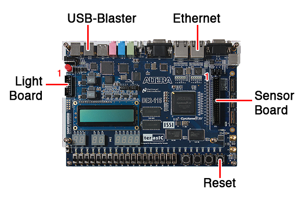
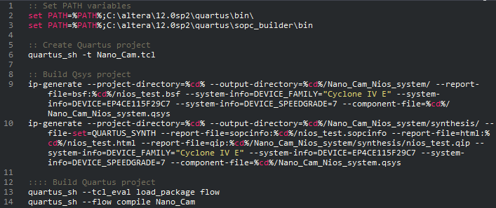
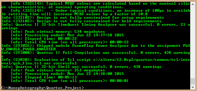
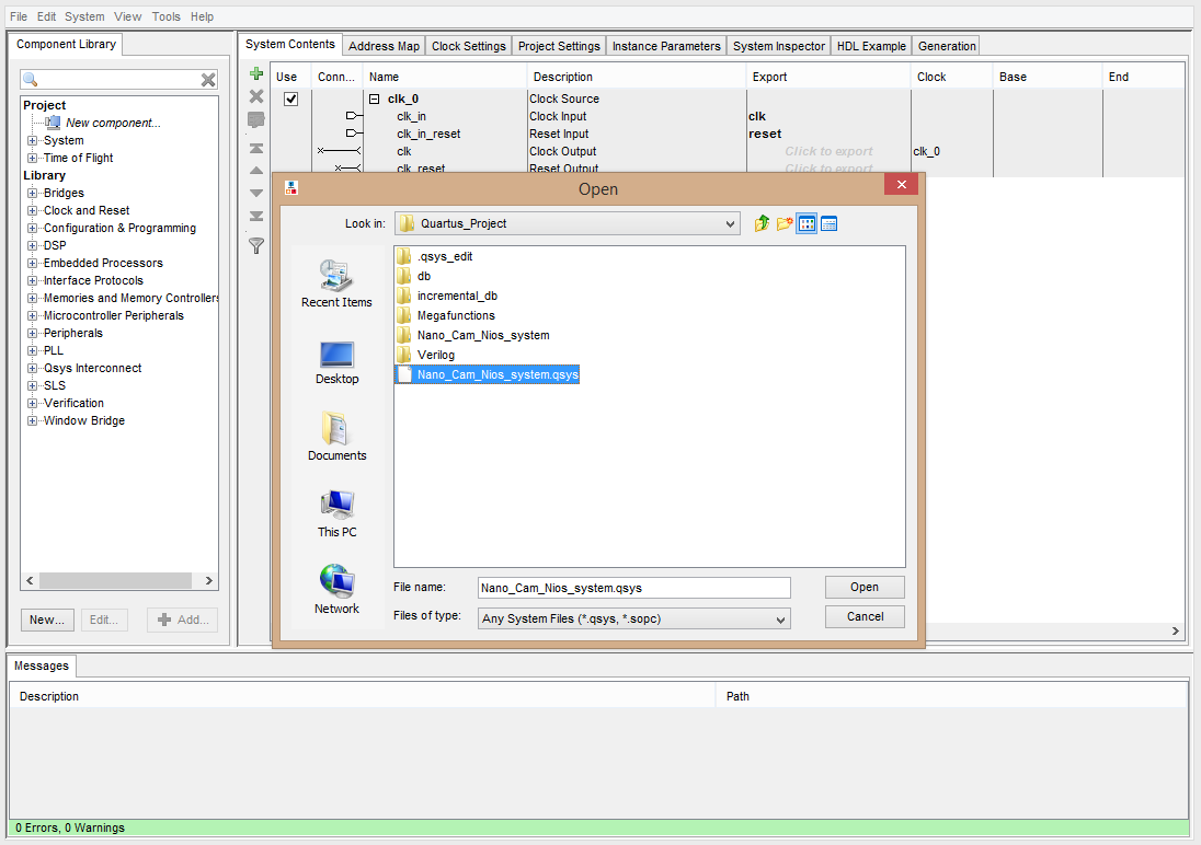
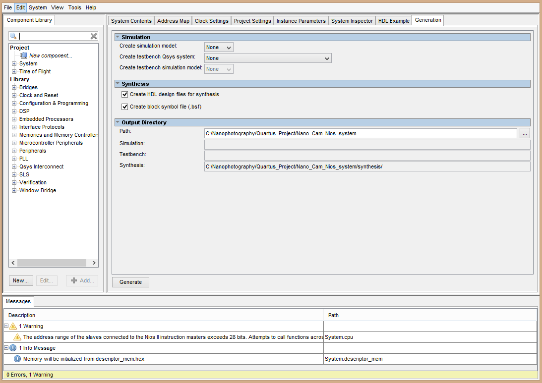
System Overview

Our camera is a time-of-flight (ToF) device. Along with capturing ultra-fast light visualizations, it can behave in more conventional ToF modes. Here, we describe the basic principles of ToF image capture and overview the building blocks of our camera. For information on the camera’s advanced functionality, beyond that of conventional devices, please refer to our Research page.

Theory of operation

The goal of ToF imaging is to recover the time it takes, `deltat`, for light to travel through a scene. From the equation `deltax = c/(deltat)`, the distance travelled, `deltax`, can be recovered and a three-dimensional map of the scene constructed.

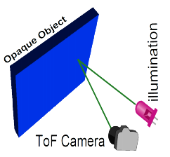
ToF cameras determine `deltat` by illuminating a scene with a strobing light source, and observing the reflected light (see left-hand figure). However, simply measuring the time delay between sending out a pulse of light and receiving a return bounce is very difficult (requiring very expensive avalanche diodes), or often even impossible with current technology (at room temperature, we quickly approach the physical limits of silicon). Instead, the conventional norm has become to measure the shift in signal phase introduced by travel time. By this approach, reflected light can be integrated over a time-period more easily achievable in modern electronics, and the time delay recovered using the equation,

`deltax = (phi/(4pi))(c/f_m)`

where `phi` is the phase delay between signals, `c` is the speed of light, and `f_m` is the modulation frequency of the signal.

Light modulation is typically implemented with either a light-emitting or fast laser diode. To determine the phase relationship between emitted and received light pulses, the electronic shutter of an image sensor is modulated in the same pattern as the light. This effectively samples the autocorrelation waveform of the modulation signal at a zero phase-offset. To sample the entire waveform, one method is to simply sweep the phase offset of the light and image sensor modulation signals through `2pi` radians. In the case of a square-wave modulation signal, the resulting correlation waveform is a sinusoid:

Phase shifting is a perfectly valid method of constructing the correlation waveform but it does not lend well to real-time capture because of the high number of samples required to accurately reconstruct the waveform (often in excess of hundreds of samples per frame). A common method for enabling real-time capture is the “four-bin” trick. In a four-bin capture, the correlation waveform is sampled at `0`, `pi/2`, `pi` and `(3pi)/2` phase offset (thereby requiring only 4 samples per frame), and the distance calculated from,

`deltax=(c/(4pif_m))tan^-1((phi_(270^o)-phi_(90^o))/(phi_(180^o)-phi_(0^o))).`

There are a whole myriad of problems lurking beneath the surface of this basic introduction to ToF imaging. For an insight into several of the major challenges, and how we’ve gone about addressing them at MIT, take a look at our Research page.

Block diagram

The diagram below depicts the data flow and important features of our camera.

FPGA & PLL: The field programmable gate array (FPGA) acts as the camera’s central computer. It generates all configuration signals to ICs, global resets, phase-shifting of modulation signals, and controls image readout through the ADC. The FPGA also contains a soft-processor that handles higher-level functionality such as memory mapping and ethernet protocol. The phase-locked-loop (PLL) sits inside the FPGA and is responsible for generating all clock signals used by the camera and FPGA. Maintaining a strict phase relationship between modulation of the image sensor’s electronic shutter and light source is particularly important, and is also achieved inside the PLLs.

PMD Image Sensor & ADC: We use a specialized ToF image sensor developed by PMD Technologies. It allows high-frequency control of the electronic shutter and fast read-out over three analog pins. Modulation of the electronic shutter is controlled by the FPGA. The analog pins are passed through an analog-to-digital converted (ADC), AD9826K, to the FPGA. The lens optics are an important design consideration not featured in the block diagram. The PMD sensor has relatively small pixel sizes so light sensitivity can often become a problem. Using a fast lens will help mitigate these effects. We currently do not recommend any specific lenses in our bill of materials, but we will in future revisions.

Illumination: Illumination is provided by 3 laser diodes. Laser diodes have superior switching speeds and brightness over LEDs, which is critical to utilising the full dynamic range of the image sensor. However, care for eye safety must always be taken when using laser diodes.

Computer: Image data is transferred to a host PC over ethernet (via a DHCP server). We provide acquisition drivers inside Matlab for grabbing data, controlling the camera, and processing raw data into light-sweep videos.

Downloads

GIT Repository

Our project is hosted on MIT’s Github, here https://github.mit.edu/schiel/Nanophotography. To clone the repository, you must first have git installed on your computer. We recommend using Github’s freely available tools as a simple interface and easy install method, available here https://windows.github.com/. To access MIT’s github, follow this guide to setup a Touchstone Collaboration account: http://kb.mit.edu/confluence/display/istcontrib/Creating+a+Touchstone+Collaboration+Account. With git installed, enter the following command in the Git shell to clone the repo:

git clone https://github.mit.edu/schiel/Nanophotography.git

The file structure should look like this:

- Matlab Drivers contains functions necessary for communicating with the camera over ethernet to change parameters and capture data.
- Nios Firmware contains the C drivers for the FPGA’s Nios soft-processor.
- PCB Designs contains the Eagle CAD files for the ToF sensor printed circuit board.
- Quartus Project contains the HDL, board-level constraints and project definitions for the FPGA project.

Quartus, Nios & Matlab

Matlab (http://www.mathworks.com/products/matlab/) is required to interface to the camera from a PC. Any moderately modern version of Matlab will work fine. Aside from a 30-day trial period, there is no free tier for Matlab. This guide assumes that you already have Matlab installed on your computer and are familiar with its basic operation.

Quartus is used to configure and flash the FPGA, and Nios is a repackaged Eclipse IDE for embedded software development. No experience with either program is required to operate or build the camera. Both packages are available for free from Altera. The camera was developed and verified with version 12.0, service pack 2, of the applications. Download v12.0 service pack 2 here: https://wl.altera.com/download/software/quartus-ii-we/12.0sp2. You will need to create an Altera account to download the software (doing so is also free of charge). Follow the website’s instructions on downloading the software. Extract the installer and launch.

The project’s automated build scripts assume that Quartus is installed in the default location, C:\altera\12.0sp2. It is not required to install the software there but if you want to use the automated build scripts you must remember to change the program location inside the git\Quartus_Project\build.bat file.

When installing the package, make sure you select to install hardware support for at least Cyclone IV devices (the FPGA used on the Terasic DE2-115 development board, which the camera uses)

The installer will install both Quartus and Nios.

Camera Hardware

This section covers the hardware setup of the camera. There are three components to the setup: 1) a field programmable gate array (FPGA) board that controls the camera and connects to a host PC, 2) a “sensor” printed circuit board (PCB) that holds the ToF sensor and ADC, 3) a “light” board that holds several laser diodes and accompanying drivers.

Eagle CAD files and a bill of materials (BOM) for manufacturing the PCBs are located in the git/PCB_Designs directory. We recommend using Digikey for component purchases, and have linked each component in the BOM to the Digikey online catalog. However, there are three items not available from Digikey: the FPGA development board, and the PMD ToF sensor, and a the laser driver. The FPGA development board should be purchased from Terasic Technologies (linked to in the BOM). The ToF die should be purchased directly from PMD Technologies. PMD does have an online store but takes orders on a case-by-case basis. Contact them for more information (contact details on the BOM). The Laser driver should be purchased from iC-Haus (https://shop.ichausamerica.com/ProductDetails.asp?ProductCode=iC-HG+EVAL+HG1D).

FPGA

Verilog modules inside the FPGA establish an interface between the PMD Sensor, ADC and PC and illumination board, controlling their operation. Detailed information on the operation of each module can be found in the commenting of each .v module file. The internal structure of the FPGA looks as follows:

  • Nano_Cam.v: Top-level design file that declares the FPGA’s I/O and instantiates the Nios soft-processor and associated drive PLL.
  • PMDAvalonWrapper.v: defines an Avalon peripheral inside the Nios soft-processor where the rest of our HDL lives. This module also defines a memory-mapped register interface for reading/writing data between the rest of the Nios soft-processor.
  • ADC_Serial_Interface.v : Defines the behaviour of a serial interface to communicate configuration information to the ADC. The ADC must be setup to sample in 3-channel sample-and-hold mode.
  • SPI.v: Standard SPI interface, used for configuring the image sensor.
  • Modulation_Controller.v: controls the modulation sequence of the lights and image sensor exposure.
  • Memory_Controller.v: instantiates FPGA dedicated RAM and controls read/write access.
  • Readout_Controller.v: Controls the sequence of operations necessary to acquire an image from the image sensor.
  • Frame_Grabber.v: Top-level controller for sending commands to the ADC serial interface and SPI, and servicing new frame requests to the readout controller.

Our FPGA of choice is the Terasic DE2-115 development board for Altera Cyclone IV FPGAs. Wiring of the board is shown below:

  • The USB-blaster is used to program the FPGA and send debugging messages.
  • Ethernet, connected to the Ethernet1 port of the board, communicates between the Nios soft-processor and Matlab.
  • Numbering of the 30-pin connector to the sensor board is the same as is shown in the Sensor Board section. The pin out of the 10-pin connector is:

Sensor board

The ToF sensor board connects to the FPGA with a 30-pin ribbon connector:

Light board

Wire the EN and GND pins to matching pins on the FPGA’s 10-pin header with jumpers. The FPGA board cannot power the light boards, so we use a desktop power supply to power the VDD rail to +5V.

Use the potentiometers on the light board to set the brightness of the laser diodes. Note that running the laser diodes at max current will cause overheating of the diodes and possible damage. We recommend operating them at a low, eye-safe current (which will also mitigate adverse temperature effects).

A fully assembled camera:

Configuring the FPGA

Bitstream synthesis is the process by which HDL is translated into a configuration understood by the FPGA to implement the desired functionality. Loading the bitstream to the FPGA is called “flashing” the FPGA. In this section, we show how to use Quartus to synthesize the provided HDL and flash the FPGA. In the first instance, we show how an included build script performs this automatically. However, we also show how to perform these tasks manually, in case the build scripts do not function correctly on your particular desktop environment, or you would like to learn the process for yourself.

The document structure of the git/Quartus_Project sub-directory should look like this:

  • NanoCam.qsf is the Quartus Settings File. It defines everything from the target FPGA, to I/O assignments, voltages and naming.
  • NanoCam.sdc is the System Device Constraints file. This file contains information about the clocking regions and timing requirements inside the FPGA design.
  • NanoCam.tcl is a Tool Command Language file that allows us to automatically rebuild the Quartus project.
  • NanoCam.v is the top-level Verilog HDL file. Here, we define the design's I/O and instantiate top-level modules such as the Nios soft-processor.
  • /Verilog sub-directory contains all of the Verilog HDL modules used by the design.
  • /Megafunctions sub-directory contains all of the Altera megablock definitions used by the designs. FPGAs have a limited number of dedicated circuits for performing certain tasks at very high data-rates. The “Megafunctions” provided by Altera allow us to instantiate these circuits from a GUI inside Quartus.
  • PMD_hw.tcl defines a hardware peripheral inside the Nios soft-processor. This is where all of our Verilog HDL lives and controls the camera.
  • build.bat is a build script for automatically invoking the TCL scripts to rebuild and synthesize the project.

Synthesizing the bitstream

The included git/Quartus_Project/build.bat script is the easiest way to synthesize the bitstream. It can be invoked by double clicking on the script inside a file explorer, or entering “build” inside a command window:

The script assumes that you installed Quartus in the default location of C:\altera\12.0sp2. If you did not install it here, you will need to open git/Quartus_Project/build.bat and edit lines 2 and 3 to your install location:

If the build was successful, you should see a series of green messages summarizing the successful build:

If this is what you see, move onto the next section “Flashing the FPGA”. If you get any error messages (which displays in red), you will need to build the project manually.

Synthesizing the bitstream manually

This sections assumes that you’ve attempted to run the build script at least once. It is important that you do so because even if it fails to synthesize the bitstream, it will still generate the needed files to open the project in Quartus and synthesize manually.

  1. Open Quartus and select File > Open Project. Open the project file git/Quartus_Project/Nano_Cam.qpf.
  2. First, we need to generate the soft-processor. Open Qsys by selecting Tools > Qsys.
  3. When prompted, select to open Nano_Cam_Nios_System.qsys
  1. Build the core by selecting the “Generation” tab, and hitting the “Generate” button.
  2. Wait for the core to finish generating, close the confirmation dialog box, select File > Save and File > Exit.
  1. Synthesize the bitstream by clicking Processing > Start Compilation
  2. When synthesis is complete, save the project by selecting File > Save Project.

Flashing the FPGA

The FPGA is flashed using the Quartus programmer:

  1. Open Quartus and select File > Open Project. Open the project file git/Quartus_Project/Nano_Cam.qpf.
  2. Open the programmer by selecting Tools > Programmer.
  3. Make sure your settings match the following:
  1. If the “Start” button is unclickable, select “Hardware Setup”. In the Hardware Setup dialog ensure that USB-Blaster is selected and then close the dialog. If there is no USB-Blaster option, you likely haven’t installed the proper blaster drivers (see Downloads section).
  1. Click “Start” to flash the FPGA.

Configuring the Processor

Firmware for the soft-processor is written to the FPGA from Nios. This section shows how to recompile the software from your git clone and upload it the FPGA. Firmware is located in the git/Nios_Firmware directory. /Nano_Cam_bsp contains the Board Support Package, and /Nano_Cam_app contains our camera application.

This section assumes that you’ve complete the Configuring the FPGA section and have the hardware setup as shown in the Camera Hardware section.

Compiling the software

  1. To build the Nios project, run the git/Nios_Firmware/build.bat script by either double-clicking the file, or calling “build” inside a command-line window. Again, if Quartus was not installed in the default location , C:\altera\12.0sp2, you will need to edit the locations in the build script:
  2. With the projects generated, open the “Nios II 12.0sp2 Software Build Tools for Eclipse” program.
  3. You will be prompted to select a workspace. Set this to the location of your Nios_Firmware folder. If you are not prompted, select File > Switch Workspace > Other to set a new one.
  4. Add the projects to the workspace by selecting File > Import. Select the “Existing Projects into Workspace” option under the “General dropdown, and select Next.
  5. Set the root directory to your Nios_Firmware folder, make sure both projects are selected, and select Finish. The Makefiles will automatically rebuild.
  6. Finally, build the project by selecting Project > Build All.

Programming the processor

  1. To program the soft-processor, we must first set up a run configuration. Select Run > Run Configurations.
  2. Select Nios II Hardware and click the page icon in the top left to create a new configuration
  1. Match the Target Configurations tab to the settings below. If no options show up in the connections, ensure you have the hardware correctly setup as outlined in Camera Hardware and have flashed the FPGA according to the Configuring the hardware section, then hit “Refresh Connections”.
  1. Hit Apply, and then Run to first save the configuration and then start it running. In the future, you now need only select Run > Run to program the soft-processor.
  2. Once the program is uploaded, it will begin executing. A terminal window will automatically open within Eclipse and show some configuration output from the Ethernet core. Note the I.P. address and port number of your camera. This will likely be different from the default I.P. addresses out Matlab drivers use, so note them for subsequent use.

Using the Camera

The camera is operated from a PC through Matlab. This guide assumes basic understanding of Matlab. The git structure looks like this:

  • NanoPhoto_connect establishes a tcpip connection to the camera.
  • NanoPhoto_set_integration_time allows image sensor exposure times to be adjusted on the fly.
  • NanoPhoto_read_image captures a single frame of raw data from the camera.
  • NanoPhoto_live_raw shows a live feed of the raw data streaming from the camera.
  • NanoPhoto_phase_step shifts the phase offset between the light source and image sensor modulation.
  • NanoPhoto_live_2D shows a live grayscale image captured by the camera.
  • NanoPhoto_capture_light_sweep captures a full set of phase images representing a light-sweep.
  • NanoPhoto_raw_to_sweep converts the raw light-sweep data into a light-sweep movie.

Real-time data visualization

Using the real-time data visualization is critical to acquiring accurate data. Use it to align and focus your optics, and make certain that light is evenly reaching the scene with adequate intensity.

A live feed of the camera’s raw data can be opened using the following command entered into Matlab’s command window:

NanoPhoto_live_raw();

The image below is an example output. Note that the fixed pattern noise is perfectly allowable because it will show up as a DC offset in the correlation waveform and is easily removed.

The second option for live data visualization shows a 2D grayscale image from the camera, using the command

NanoPhoto_live_2D();

An example output is shown below.

Capturing a light-sweep

Light-sweeps are captured using the command

NanoPhoto_capture_sweep (steps, avg);

The “steps” input defines the number of phase steps need to capture a full sweep. For the default settings, as cloned from the git repo, this will be 3350 steps. However, if you change the modulation frequency, you will need to adjust the number of steps accordingly to ensure an entire sweep is still captured.

“avg” sets the number of samples to take at each phase step. We recommend at least 5 samples. More samples will give more accurate data but increase the acquisition time.

The output of capturing a light sweep is an 120x160x(steps)-sized array (120x160 is the resolution of each image frame). Plotting a pixel location along the third dimension (phase) shows the correlation waveform at that point in the scene:

To convert this data to a light-sweep video, call the function

NanoPhoto_raw_to_lightsweep (frames);

The movie will automatically play, and be output by the function.